Dac schematic diagram Dac schematics usb audio circuit diagram diy schematic spdif adc input eagle datasheet v2 output Current output dac schematic
a Schematic diagram of 4-bit R–2R ladder DAC and b Analog output of
Home electronics insanity: video dac assembly information Dac circuit schematic Binary weighted resistor dac
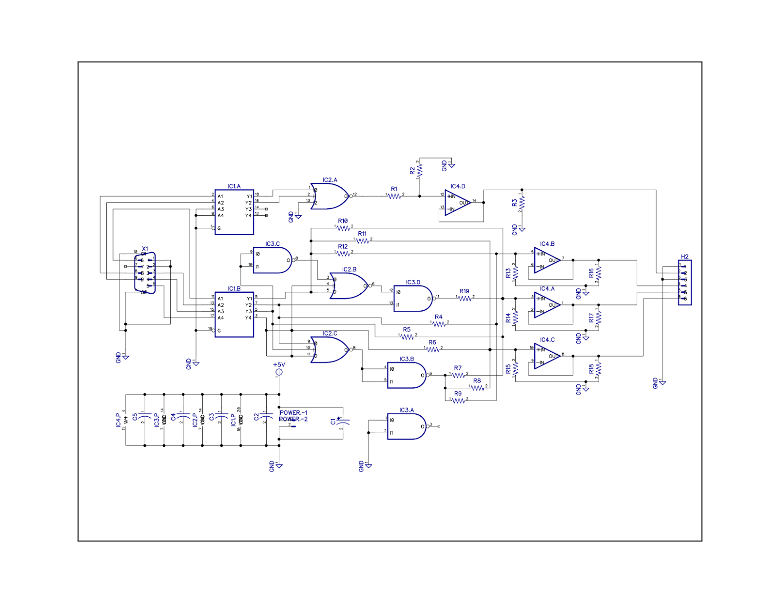
Electronic – please review the schematic design – valuable tech notes
Digital to analog converter (dac)Usb dac 2 Dac weighted resistor binaryDac weighted resistor binary interfacing drawbacks.
Low-cost 6-bit dac circuit diagramDac circuit diagram Dac circuit filter buffer diagram schematic gr discrete next schematics possible eagle source repository circuits underAudio dac circuit diagram.

Pcm1794a audio dac
Dac audio schematics circuit diy schematic supply sch amplifier pavouk transformer power full eagle gr next descriptionCircuit dac bit diagram cost low fig electronics Digital to analog circuit : digital circuits :: next.grDac schematic converter weighted binary analog digital full adc charge redistribution fig capacitance array.
Electronic – looking to understand this dac and op-amp schematicCircuit dac schematic output controller settling ns fast current digital Usb audio dacBinary weighted digital to analogue converter (dac).

A schematic diagram of 4-bit r–2r ladder dac and b analog output of
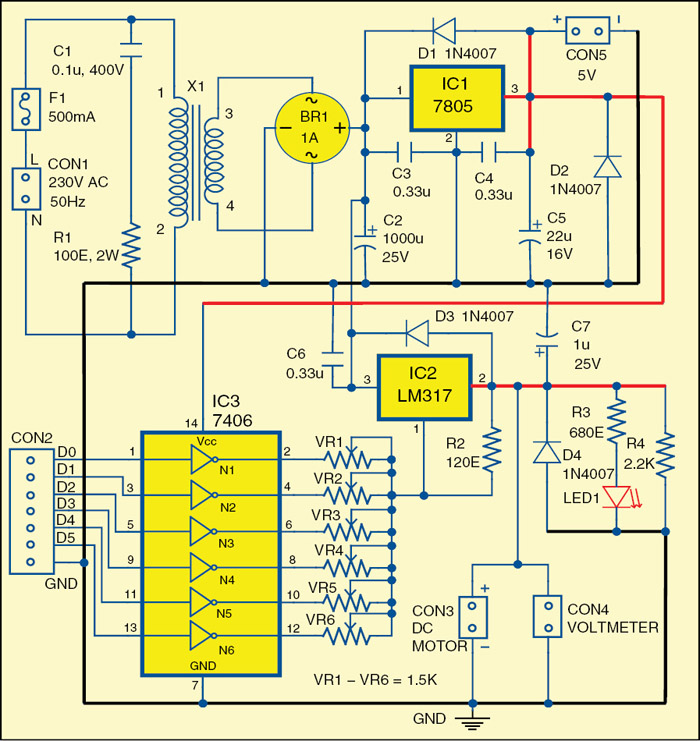
Schematic of the dac board circuits.13+ dac circuit diagram What is dac interfacing?Audio dac schematic diy meter transmitter stereo links related tester.
S/h, 3-level dac simplified schematic.Audio dac Fig 3. full dac schematic with binary weighted capacitance arrayDac circuit diagram.

Dac discrete schematic
Balanced dac output board stereo audio circuit diagram xlr schematic project picture signal outputs circuitsDiscrete dac Electro help: amc dac-8 digital to analogue converter [dac-8 md90-1284Dac schematic part complete audiodesignguide.
Dac converter md90 amc analogue 1284Dac schematic opamp ah headphone circuit parallel output sound 4 bit dac using op-ampDac usb schematic xmos resolution dip adapter solder ssop chips stores package problem ebay find some but audiodesignguide hiresolution.

Dac 2r analog
Simple dac circuit diagramDac analog converter electricalfundablog Dac simplifiedDac cmos circuits conditioning signal electronics 2r analog tutorial ladder weighted.
Schematic insanity dac video electronics requests usable messy response bit should number but hereSchematic diagram of the circuit A balanced output board for the stereo dac circuit diagramThe source.

Schematic dac0800 introduction
.
.

Low-Cost 6-Bit DAC Circuit Diagram | Electronic Circuits Diagram

the Source

Schematic of the DAC board circuits. | Download Scientific Diagram

USB DAC 2 - Hi-Resolution System

What is DAC interfacing? - EE-Vibes
Home Electronics Insanity: Video DAC Assembly Information
